Facilities and Tools
Epitaxy of thin films and heterostructures
Pulsed Laser Deposition (PLD)
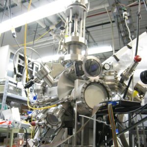
A cluster of 10 conventional PLD systems is available to grow complex oxide thin films and heterostructures. These systems each have multitarget carousels (up to 4) and are part of a cluster of deposition chambers sourced by a 50 W (at 50 Hz) Coherent KrF excimer laser (model LPX Pro 305) or a 30 W (at 50 Hz) Coherent KrF excimer laser (COMPexPro 205). All chambers have motioncontrolled target carousels responsible for automatic target clocking during multilayer growth and target rastering during ablation to promote uniform target erosion. Each system is equipped with an oxygen compatible heater (~ 900 ºC maximum) for deposition in vacuum, inert, and reactive ambient. Mass flow controllers and a downstream throttle valve are employed to adjust the gaseous film-growth environment. A part of the systems is designed for quick discovery of new materials with RHEED designed to provide in situ growth monitoring capability available for controlled growth of thin films and multilayers.
Contact me for more details or collaborations.
Molecular Beam Epitaxy (MBE)
Three MBE system focusing on separate chemistries specifically chalcogenide and oxides:
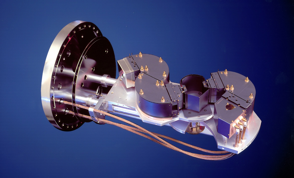
Chalcogenide MBE: chalcogenide-based system equipped with 6 conventional effusion cells with maximum temperature ranging from 100-2000 °C; in situ characterization is provided in real time through RHEED, spectroscopic ellipsometry, quadrupole residual gas analyzer, and in situ flux calibration utilizing a quart crystal microbalance. Substrate heating is provided by a radiative filament heater capable of temperatures in excess of 1000 °C.
Intermetallic MBE: Intermetallic MBE equipped with 7 conventional effusion cells with temperature ranging from 100-2000 °C, and large multipocket e-beam evaporation cell enabling use of refractor elements such as Zr-Ru, Hf-Pt. In situ characterization is provided in real time through RHEED, quadrupole residual gas analyzer, spectroscopic ellipsometry, and in situ flux calibration utilizing a quart crystal microbalance. Substrate heating is provided by a radiative filament heater capable of temperatures in excess of 1000 °C.
Oxide MBE: oxide MBE equipped with 7 conventional effusion cells with maximum temperature ranging from 100-2000 °C, and an e-beam evaporation cell enabling use of refractor elements such as Zr-Ru, Hf-Pt; an RF oxygen plasma source for highly reactive atomic oxygen; in situ characterization is provided in real time through a high-pressure differentially pumped RHEED, Auger spectroscopy, quadrupole residual gas analyzer, and in situ flux calibration utilizing a quart crystal microbalance. Substrate heating is provided by a laser heater capable of temperatures in excess of 1200 °C.
Contact Matt Brahlek or me for more details or collaborations.
RF Magnetron Sputtering
A RF magnetron sputtering system (built in-house) is used for conventional and reactive deposition. The facility is all-manual except for rate monitoring, utilizes three 1-inch targets, and can accommodate substrates up to 4 inches in diameter. The system is presently configured for deposition of Pt, Ti, Cr, and Au, but other materials are possible and only dependent on the availability of targets.
Characterization and Testing Equipment
Spin- and Angle-Resolved Photoemission Spectroscopy (S-ARPES)
State-of-the-art spin- and angle-resolved photoemission spectroscopy (ARPES) to provide rapid prototyping and electronic structure characterization of both thin film and bulk topological materials. This system is also being configured for laser APPES (11 eV). The following specs are available for studying various types of quantum materials. Contact Rob Moore or Hu Miao for more details.
· Electrostatic lens system for mapping the electronic structure through the momentum space
· Two orthogonal very low-energy electron diffraction (VLEED) spin detectors.
· 11 eV laser (Oxide) and VUV He lamp light with photon flux densities ~2e+12 photons/s/mm
High-Resolution Momentum-Resolved Electron-Energy Loss Spectroscopy (HR-MEELS)
A HR-MEELS that is directly connected to the ARPES chamber is being developed and is expected to be ready by summer 2021. This unique capability allows us simultaneously characterizing the surface electronic band, plasmon, phonon and magnon excitations with the same Scienta Omicron DA-30 electron analyzer. The LK5000M electron source from LK technology has double pass electron monochromator with internal magnetic shielding, subchamber and transfer lens and can reach energy resolution (full-width-at-half-maximum) better than 2.5 meV in normal operation conductions with output current better than 200 pA. The system can be operated for 0-250 eV kinetic energy, which can cover large momentum space
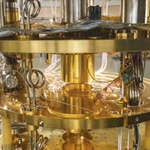
mK Microscopy for QIS
A milliKelvin microscopy platform was installed in 2019 that integrates a confocal optical microscope and atomic force microscopes from Nanomagnetics Instruments into a closed cycle Leiden Cryogenics LC CF‐CS81‐1400‐Maglev dilution refrigerator. The dilution refrigerator has a base temperature of 10 mK and cooling power of 1mW at 100mK. A cold insertable probe allows for samples and microscopes to be removed from the fridge and modified or exchanged while the fridge is held at liquid helium temperatures. The cold insertable probe allows for faster sample throughput with a higher base temperature of 20mK and a cooling power of 200µW at 100mK. A free-space clear-shot to the mixing chamber, together with a galvo scanner and an 8f imaging system enables high speed optical imaging, microscopy, and spectroscopy at mK temperatures. Tuning fork and cantilever based atomic force microscopes can be mounted in place of the confocal microscope for milliKelvin scanning probe microscopy, and dual-probe head now integrates a confocal microscope stage and a tuning fork AFM stage for preliminary milliKelvin scanning NV magnetometry. It is equipped with a vector magnet with 6/1/1T field.
Contact Ben Lawrie for more details or collaborations.
Dynamic X-ray Photoemission Spectroscopy (XPS)
A Sigma Pulse dynamic XPS system is capable of both, in situ characterization of films grown and transferred from the growth system, and stand-alone real-time measurements of peak-intensities during surface modifications and transformations occurring independently in the characterization chamber. The fast data acquisition is enabled by a 160 mm radius Aspect hemispherical energy analyzer with a high transmission fast electronics and a true counting multichannel detector. The operation of the analyzer and the X-ray sources is fully integrated by the control and the data acquisition software.
Contact Gyula Eres for details or collaborations.
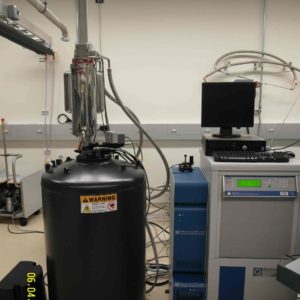
Quantum Transport
An oxford dilution fridge with 5 mK base temperature and ±14 T with two-axis sample rotation is available for quantum transport measurements and mapping Fermi surfaces. Electrical inputs/outputs (I/Os) span 0Ω to 1 TΩ, and DC to 20 GHz. Measurement modalities include: de Haas–van Alphen (dHvA) and Shubnikov–de Haas (SdH) oscillation mapping, base resistivity, gating responses, torque magnetometry.
Contact me for more details or collaborations.
Physical Properties Measurement Systems (PPMS)
Two Quantum Design Physical Properties Measurement Systems (PPMS) with 9 and 14 T magnets can measure specific heat, resistivity, thermopower, thermal conductivity, and Hall coefficient in the temperature range of 1.9-400K. The 14 T PPMS is equipped with a He re-liquefier, VSM, and dilution refrigerator. The latter enables the system to measure heat capacitance and electric transport down to 50 mK. The PPMS system is also equipped with a Keithley 6514 Programmable Electrometer for high resistance measurements (> 200 TW) and an AC and DC Current Source (Keithley 6221) featuring exceptionally low current noise.
Contact me for more details or collaborations.
Magnetic Properties Measurement Systems (MPMS)
A Quantum Design Magnetic Properties Measurement System 3 (MPMS 3, VSM-SQUID) is also available for magnetic measurements. This cryogen free system with evercool incorporates major advances in data acquisition, temperature control (1.8-400K), and magnetic field control (7 T) with up to 10-8 emu sensitivity.
Contact me for more details or collaborations.
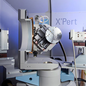
X-ray diffraction
Two high-resolution four-circle x-ray diffractometers (X’Pert Pro, PANalytical) equipped with Ge monochromators is available for analyzing phase, orientation, stress, texture, crystallography, and structure of various material classes with Cu-Ka1 radiation. These systems handle wafers up to 4 inches in diameter and can expedite the measurements by mounting many small-sized samples at a time for programmed measurements. A sample holder for bulk or power samples is also available, and both systems have a 1D hybrid pixel detector for fast high precision measurements. The diffractometer is equipped with an automatic attenuator for reducing the risk of accidental exposure of the detector to high x-ray counts while maintaining a high sensitivity of reflected beams from thin film samples. One of the two systems has a DHS1100 graphite domed high temperature stage to measure XRD up to 1100 oC. The ICDD Power Diffraction Database is installed covering more than 115,000 compounds.
Contact me for more details or collaborations.
Thermal characterization and spectroscopy
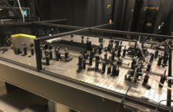
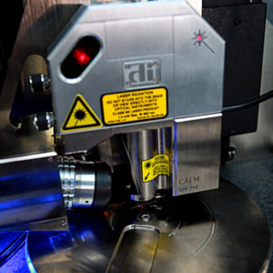
Time Domain Thermoreflectance (TDTR) offers the capability for non-contact and non-invasive probe of both cross- and in-plane thermal conductivities in a variety of materials. The operating temperature varies from 4 to 400 K. This apparatus can be readily converted into a thermal conductivity imaging instrument for studies of spatially heterogeneous materials.
Transient Thermal Grating (TTG) spectroscopy probes the thermal response of a material subject to spatially periodic heating from time-coincident coherent laser pump pulses crossed to form an interference pattern with period L. This leads to a periodic temperature response at the sample surface, or “transient grating”. The decay of this temperature profile by transport processes is monitored via diffraction of a probe laser beam and gives information for extracting thermal properties of the material. The operating temperature ranges from 4 to 400 K.
Transient Absorption Spectroscopy (TAS) probes the time-resolved spectrum of the ultrafast dynamics of photoexcited hot carriers. A 50-fs pump pulse centered at 500 nm was used to excite carriers well above the band gap for both samples, while an ultrashort broadband white-light continuum (480 – 1100 nm) was used as probe. The pump-induced change in absorbance is then acquired as a function of time delay, which contains information regarding inter-system crossing, intermediate unstable electronic states, trap states, surface states etc.
Contact Chengyun Hua for more details or collaborations.
Atomic force Microscopy (AFM)
A Digital Instruments system is used for micro- and nanoscale surface imaging and metrology. The Dimension 3100 SPM handles a wide range of sample sizes up to 6-in diameter and 12 mm thick. The system is configured currently with a standard scanner that not only maintains extremely low noise levels (<0.5 Å rms Z, <2 nm rms XY, with present acoustic and vibrational isolation), but utilizes patented TrakScan technology to maintain precise positioning of the laser on the cantilever during scanning. The Nanoscope IIIa controller enables scan areas that range from a few nm to nearly 100 mm on each axis, and this area can be positioned precisely over a 125 ´ 100-mm inspection area with better than 5-mm repeatability. The atomic force microscopy (AFM) system has also been used for local piezoresponse and conductance measurements (i.e., as PFM and C-AFM).
Contact me for more details or collaborations.
Lithography and Device Fabrication
A UV photolithographic lift-off capability is available for device fabrication. A RF sputter and a wire bonder are also available for metal deposition and wiring contact leads, respectively.
Contact me for more details or collaborations.
Electrical, Optical, and Dielectric Characterization Tools
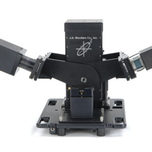
in situ Ellipsometry – The JA Woollam M-2000U of spectroscopic ellipsometer is used for analysis of the optical properties of thin films and Heterostructures. This system is configured in a PLD chamber for in situ and in operando optical characterization.
– 210 – 1690 nm spectral range and 675 wavelengths measured simultaneously
– Minimum data acquisition time approximately 50 msec
– Typical data acquisition times 1-5 sec
– Collimated light beam (diameter varies with model: 2-5 mm)
– NIR Upgraded – extends upper wavelength limit to 1690nm
– Test base for ex situ testing; angles of incidence: 65° & straight-through (90°), horizontal sample stage
Ferroelectric tester – TF 2000, aixACCT Systems with a frequency range from 1 mHz to 2 MHz is available. Standard features include hysteresis, pulse response, fatigue, retention, and imprint measurements essential for ferroelectric memory applications. Two external voltage sources are available and can extend the TF’s internal voltage source of 24 to 200 V and 10 kV. A probe station including two micromanipulators and an optical microscopy with a CCD camera attached is also available.
Capacitance and dielectric loss as a function of temperature can be measured from 35 to 400 K and as a function of frequency from 20 Hz to 1 MHz up to 30 V of DC bias.
Contact me for more details or collaborations.